


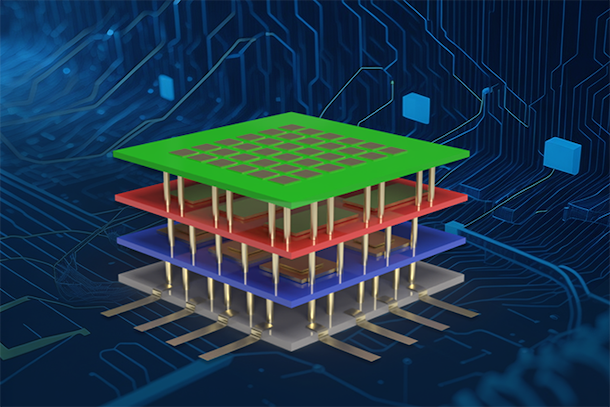
Penn State researchers demonstrated 3D integration of semiconductors at a massive scale, characterizing tens of thousands of devices using 2D transistors made with 2D semiconductors, enabling electronic gadgets to possibly become smarter and more versatile. Credit: Elizabeth Flores-Gomez Murray/Materials Research Institute. All Rights Reserved.
Integrating dimensions to get more out of Moore’s Law and advance electronics
January 10, 2024
By Jamie Oberdick and Ashley WennersHerron
Editor's note: This article originally appeared on Penn State News.
UNIVERSITY PARK, Pa. — Moore's Law, a fundamental scaling principle for electronic devices, forecasts that the number of transistors on a chip will double every two years, ensuring more computing power — but a limit exists.
Today's most advanced chips house nearly 50 billion transistors within a space no larger than your thumbnail. The task of cramming even more transistors into that confined area has become more and more difficult, according to Penn State researchers.
In a study published today (Jan. 10) in the journal Nature, Saptarshi Das, an associate professor of engineering science and mechanics and co-corresponding author of the study, and his team suggest a remedy: seamlessly implementing 3D integration with 2D materials.
In the semiconductor world, 3D integration means vertically stacking multiple layers of semiconductor devices. This approach not only facilitates the packing of more silicon-based transistors onto a computer chip, commonly referred to as “More Moore,” but also permits the use of transistors made from 2D materials to incorporate diverse functionalities within various layers of the stack, a concept known as “More than Moore.”
With the work outlined in the study, Saptarshi and the team demonstrate feasible paths beyond scaling current tech to achieve both More Moore and More than Moore through monolithic 3D integration. Monolithic 3D integration is a fabrication process wherein researchers directly make the devices on the one below, as compared to the traditional process of stacking independently fabricated layers.
“Monolithic 3D integration offers the highest density of vertical connections as it does not rely on bonding of two pre-patterned chips — which would require microbumps where two chips are bonded together — so you have more space to make connections,” said Najam Sakib, graduate research assistant in engineering science and mechanics and co-author of the study.
Monolithic 3D integration faces significant challenges, though, according to Darsith Jayachandran, graduate research assistant in engineering science and mechanics and co-corresponding author of the study, since conventional silicon components would melt under the processing temperatures.
“One challenge is the process temperature ceiling of 450 degrees Celsius (C) for back-end integration for silicon-based chips — our monolithic 3D integration approach drops that temperate significantly to less than 200 C,” Jayachandran said, explaining that the process temperature ceiling is the maximum temperature allowed before damaging the prefabricated structures. “Incompatible process temperature budgets make monolithic 3D integration challenging with silicon chips, but 2D materials can withstand temperatures needed for the process.”
The researchers used existing techniques for their approach, but they are the first to successfully achieve monolithic 3D integration at this scale using 2D transistors made with 2D semiconductors called transition metal dichalcogenides.
The ability to vertically stack the devices in 3D integration also enabled more energy-efficient computing because it solved a surprising problem for such tiny things as transistors on a computer chip: distance.
"By stacking devices vertically on top of each other, you're decreasing the distance between devices, and therefore, you're decreasing the lag and also the power consumption,” said Rahul Pendurthi, graduate research assistant in engineering science and mechanics and co-corresponding author of the study.
By decreasing the distance between devices, the researchers achieved “More Moore.” By incorporating transistors made with 2D materials, the researchers met the “More than Moore” criterion as well. The 2D materials are known for their unique electronic and optical properties, including sensitivity to light, which makes these materials ideal as sensors. This is useful, the researchers said, as the number of connected devices and edge devices — things like smartphones or wireless home weather stations that gather data on the ‘edge’ of a network — continue to increase.
"’More Than Moore’ refers to a concept in the tech world where we are not just making computer chips smaller and faster, but also with more functionalities,” said Muhtasim Ul Karim Sadaf, graduate research assistant in engineering science and mechanics and co-author of the study. “It is about adding new and useful features to our electronic devices, like better sensors, improved battery management or other special functions, to make our gadgets smarter and more versatile.”
Using 2D devices for 3D integration has several other advantages, the researchers said. One is superior carrier mobility, which refers to how an electrical charge is carried in semiconductor materials. Another is being ultra-thin, enabling the researchers to fit more transistors on each tier of the 3D integration and enable more computing power.
While most academic research involves small-scale prototypes, this study demonstrated 3D integration at a massive scale, characterizing tens of thousands of devices. According to Das, this achievement bridges the gap between academia and industry and could lead to future partnerships where industry leverages Penn State’s 2D materials expertise and facilities. The advance in scaling was enabled by the availability of high-quality, wafer-scale transition metal dichalcogenides developed by researchers at Penn State's Two-Dimensional Crystal Consortium (2DCC-MIP), a U.S. National Science Foundation (NSF) Materials Innovation Platform and national user facility.
"This breakthrough demonstrates yet again the essential role of materials research as the foundation of the semiconductor industry and U.S. competitiveness," said Charles Ying, program director for NSF's Materials Innovation Platforms. "Years of effort by Penn State's Two-Dimensional Crystal Consortium to improve the quality and size of 2D materials have made it possible to achieve 3D integration of semiconductors at a size that can be transformative for electronics."
According to Das, this technological advancement is only the first step.
"Our ability to demonstrate, at wafer scale, a huge number of devices shows that we have been able to translate this research to a scale which can be appreciated by the semiconductor industry,” Das said. “We have put 30,000 transistors in each tier, which may be a record number. This puts Penn State in a very unique position to lead some of the work and partner with the U.S. semiconductor industry in advancing this research.”
Along with Das, Jayachandran, Pendurthi, Sadaf and Sakib, other authors include Andrew Pannone, doctoral student in engineering science and mechanics; Chen Chen, assistant research professor in 2DCC-MIP; Ying Han, postdoctoral researcher in mechanical engineering; Nicholas Trainor, doctoral student in materials science and engineering; Shalini Kumari, postdoctoral scholar; Thomas McKnight, doctoral student in materials science and engineering; Joan Redwing, director of the 2DCC-MIP and distinguished professor of materials science and engineering and of electrical engineering; and Yang Yang, assistant professor of engineering science and mechanics.
The NSF and Army Research Office supported this research.