


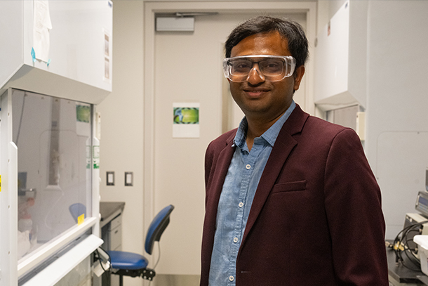
Saptarshi Das will lead a multi-institution team to develop an all-in-one semiconductor device that can both store data and perform computations. Credit: Tyler Henderson/Penn State
Project aims to develop all-in-one semiconductor that stores, processes data
October 3, 2023
By Ashley WennersHerron
Editor’s note: This story originally appeared on Penn State News.
UNIVERSITY PARK, Pa. — A multi-institutional project led by a Penn State researcher is focused on developing an all-in-one semiconductor device that can both store data and perform computations. The project recently received $2 million in funding over three years as part of the new National Science Foundation Future of Semiconductors (FuSe) program, a $45.6 million investment to advance semiconductor technologies and manufacturing through 24 research and education projects across the United States.
“The goal of the program is to support innovation in semiconductors, which we need to address rapidly approaching limitations of current technology,” said principal investigator Saptarshi Das, associate professor of engineering science and mechanics in Penn State’s College of Engineering.
Microchip technology, crucial for computing and data storage in a wide range of advanced devices from smartphones to electric vehicles, has historically advanced to accommodate a doubling of transistor capacity approximately every two years. This phenomenon is known as Moore's Law. However, Moore's Law reached a standstill almost a decade ago, constrained by what Das called the inherent limitations of the prevailing materials and techniques.
According to Das, stagnation in Moore’s Law only accounts for making the transistors smaller.
“Another major problem in the semiconductor architecture is you have to get data from the memory, make the computation and put the data back,” Das said. “This shuttling consumes a lot of power. Can we do it in the same device?”
Das teamed up with co-principal investigators Ritesh Agarwal, professor of materials engineering, and Deep Jariwala, associate professor of electrical systems engineering, both at the University of Pennsylvania. Agarwal and Jariwala had developed new semiconducting materials comprising various phases of indium selenide that Das said they thought might be able to bridge the gap between storage and computation in a single device.
To help address how transistors based on these novel materials might fit into the existing confines of technology, they brought in Priyadarshini Panda, assistant professor of electrical engineering at Yale University, who specializes in artificial intelligence and its application across full systems — in other words, if the team develops a singular, multifunction semiconductor device, how will it operate at the system level with other such devices?
“It’s not just the material or just the device — every piece has to come together for the project to be successful,” said Das, who is an expert in neuromorphic computing, or engineering computational elements that model the human brain. “We could make a champion device but if it doesn’t fit in a system, it doesn’t work. That is why we need this full team, with complementary expertise.”
The semiconducting material developed by the University of Pennsylvania team is ferroelectric, meaning it holds an electric charge that can be flipped if a voltage is applied. It’s unusual for a material to be both ferroelectric and semiconducting, Das said.
“Ferroelectric materials are dipoles, pointing up or down, that can be changed by applying a voltage — it’s a natural storage device with two stages,” Das said, explaining that it is comparable to binary code, the ones and zeroes that serve as the underlying architecture for modern computing. “Ferroelectric materials typically can’t be gated — or partially turned off — like semiconductors, when you stop the material’s conductance to control information or energy flow. But this ferroelectric material is a semiconductor, so it can be gated.”
The researchers said they plan to use this material to develop a new two-in-one storage and computing device that can integrate with standard silicon chips at the back end. This would help with quicker implementation, since the new devices could work with existing systems, according to Das. That would also set the stage for developing and manufacturing more neuromorphic computing devices, which mimic the energy saving and unique storage abilities of the human brain.
“This material will let us capture the best of both worlds: storage and computation,” Das said. “That opens up the possibilities, and that’s why we’re so excited about this project.”
The funding will also support four students, one per collaborator, to work on this project.
"Our investment will help train the next generation of talent necessary to fill key openings in the semiconductor industry and grow our economy from the middle out and bottom up," said NSF Director Sethuraman Panchanathan in a statement. "By supporting novel, transdisciplinary research, we will enable breakthroughs in semiconductors and microelectronics and address the national need for a reliable, secure supply of innovative semiconductor technologies, systems and professionals."
Das is also affiliated with the Materials Research Institute and the Center for Neural Engineering and holds courtesy appointments in materials science and engineering and in electrical engineering and computer science.