


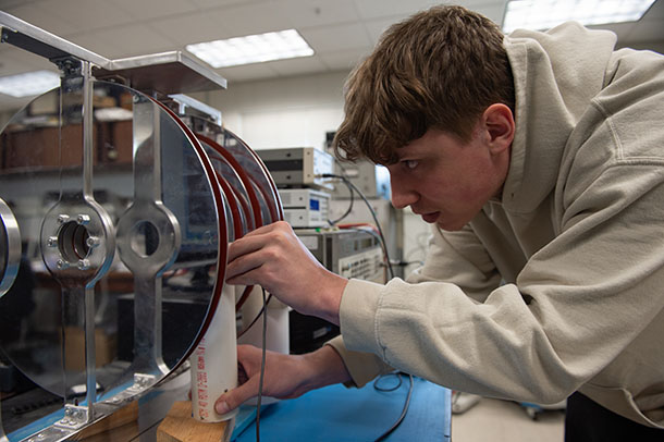
Engineering science and mechanics doctoral student Fedor Sharov adjusts settings in a very low frequency EDMR spectrometer. Credit: Kelby Hochreither/Penn State. All Rights Reserved.
New tool measures atomic scale defects, identifies transistor limitations
The approach may enable advanced electronic devices, researchers say
May 23, 2022
By Sarah Small
UNIVERSITY PARK, Pa. — A new technique for studying defects in semiconductor materials could lead to improved speed, power and performance of electronic devices by revealing the atomic-level limitations of advanced materials.
Developed by a Penn State-led team of researchers and lead by former Penn State graduate student James Ashton, the analytic tool makes use of extremely small magnetic fields and frequencies far smaller than those typically used in such measurements to detect and measure imperfections in new materials, providing structural information about the magnetic interactions between electrons and nearby magnetic nuclei in a simpler way than previously possible.
The approach was published as a cover article in Applied Physics Letters. According to Patrick Lenahan, distinguished professor of engineering science and mechanics at Penn State and Ashton’s doctoral thesis adviser, the tool allows researchers to take a big step toward solving a variety of faults in next-generation devices.
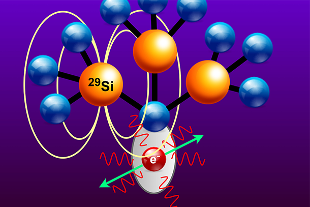
The work was featured as the cover of the Applied Physics Letters of the issue in which it appeared. Credit: Provided by Patrick Lenahan. All Rights Reserved.
The researchers focused on metal oxide semiconductor field effect transistors (MOSFETs), which are found in nearly every device with integrated circuits, from cell phones to computers. Previously designed with silicon and silicon dioxide, MOSFETs now can be fabricated with other materials, including silicon carbide as the semiconducting material. Lenahan pointed out that the relatively new material has substantial advantages for high temperatures and high power applications. However, he explained, silicon carbide MOSFETs are limited by atomic scale defects which researchers have not been able to fully understand.
“The presence of one subtle defect, like a missing atom site per every, say, 5,000 atoms at the boundary between the silicon carbide and the MOSFET gate oxide, will be enough to ruin any device,” Lenahan said. “So, we needed a way to look at the subtle deviation from perfection, to understand what is limiting the performance of these devices.”
To detect such deviations, researchers use magnetic resonance — similar to the technology clinicians use to visualize soft tissue abnormalities in the human body — to excite electrons in SiC MOSFETs. These measurements can give detailed information about the material’s imperfections, particularly where the electrons interact with atomic scale imperfections such as missing atom sites. Traditionally, this technique required a high magnetic field and had a sensitivity of about 10 billion defects — far more defects than those present in the small SiC devices. Recently, however, a newer iteration of the technique, called electrically detected magnetic resonance, has emerged, for which the size of the field is irrelevant to sensitivity and a much smaller of device-limiting defects could be directly detected during electrical operation, according to Lenahan.
“The fact that you can make extremely sensitive magnetic resonance work with extremely small magnetic fields is an area which is basically not investigated at all,” Lenahan said. “Theorists have written papers asking, ‘Suppose you could make such a measurement — what might you find out?’ And it turns out that there is a way, which is what we’ve demonstrated here with our new analytical tool.”
Lenahan, Ashton and their team applied electrically detected magnetic resonance to measure the effects of spin on atomic scale interactions captured at an imperfection in a device using extraordinarily small magnetic fields.
Spin describes a fundamental characteristic of particles such as electrons protons and neutrons. All electrons, including those captured at the imperfections in MOSFETs, have spin, and the nuclei of atoms surrounding them can also have their own spin. Electrically detected magnetic resonance can measure the ‘hyperfine interactions,’ which are the magnetic interactions between the electron and nuclear spins. Observing these interactions can reveal structural and chemical details about these defects.
“People have been interested in electron-nuclear hyperfine interactions for over 60 years, and this tool provides a new way to look at these interactions in very small samples with an electrical measurement,” Lenahan said. “We're looking at nanometer by micron-by-micron samples — samples that are billions of times smaller than what you could investigate with more conventional resonance techniques — so we can really understand on an atomic level what it is that limits the performance of this particular device. From that understanding, we can suggest how people in industrial research and development labs might try to make the devices work better.”
According to Stephen Moxim, a co-author on the publication and Penn State engineering science and mechanics doctoral student, the results also relate to more fundamental spin physics.
“When electron spins within defect centers ‘flip,’ or change their spin state, in a magnetic resonance experiment, they eventually relax back to their original spin state,” he said. “Among other things, the results here show how this relaxation process is related to the environment in which the defects exist. Specifically, they give us an idea of how the magnetic nuclei sitting near the defect electrons affect the relaxation process.”
According to Moxim, this approach, built on a relatively simple direct electrical current measurement tool, could potentially translate to the field of quantum computing.
“It is always incredible when you see the intersection of theoretical physics and practical engineering,” said Fedor Sharov, co-author and Penn State engineering science and mechanics doctoral student. “Ideas and theory from decades ago are finding a perfect home in a new technique that, in the recent past, theorists might not have even considered.”
Other authors on the paper are Brian Manning, of Keysight High Frequency Technology Center in Santa Rosa, California,where Ashon now works, and also a doctoral student of Lenahan during some of this research ; and Jason Ryan, a project leader at the National Institute of Standards and Technology (NIST) and Ashton’s adviser during his time at NIST, who also earned his doctorate in the Lenahan group.
The U.S. Army Research Laboratory and the Air Force Office of Scientific Research funded this work.