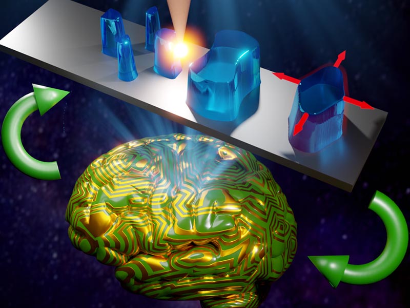
Deep learning, represented by the brain in this illustration, can accelerate the optimization of robust nanostructures, paving the way for optical metasurfaces that can tolerate a range of manufacturing defects. IMAGE: RONALD JENKINS
Deep learning to make nanoscale designs more robust against defects
12/9/2021
By Gabrielle Stewart
UNIVERSITY PARK, Pa. — Optical metasurfaces, ultrathin interfaces made up of uniform nanoscale structures, change the behavior of light waves hitting them to produce effects ranging from unique reflection and transmission properties to lens distortion removal. However, due to the small size of metasurface features, manufacturing defects can significantly reduce performance — and they are hard to anticipate.
A team of Penn State researchers developed a method to account for the effect of small defects before they’ve occurred to enable designs that can withstand these performance reductions. They published their approach in Nanophotonics in November.
“With modern nanofabrication technology, superfine features — or small structures inside metasurface components — can be made consistently, but this can affect the processing time,” said Ronald Jenkins, an electrical engineering doctoral candidate and first author on the paper. “The goal of this research was to identify a method that would allow design of structures that can tolerate those inevitable defects and still perform well.”
The researchers first used an optimizer, software that virtually tests different designs and suggests new variations based on the most successful configurations, to generate metasurface designs. A restriction on the minimum feature sizes in these metasurface components, or unit cells, could be imposed by the researcher based on the limitations of the targeted nanofabrication technique.
Once the optimizer had determined unit cell forms with good performance, these data were used as inputs in a deep learning model. The model had been trained to predict how inevitable manufacturing defects would affect performance using data from highly accurate, electromagnetic modeling software tools. With the optimizer’s inputs, the deep learning model applied its trained knowledge of how defects influence performance to determine the optimized designs’ robustness to those defects. This assessment was then fed to the optimizer, which generated high-performance designs that could withstand the effect of manufacturing defects as described by the deep learning model.
With this feedback loop, the researchers can apply the benefits of the more expansive algorithms without running them, which would be too expensive and time-consuming to run on a scale that supports manufacturing, according to Jenkins.
“It would take an overwhelming computational load to complete both design optimization and integration of the uncertainty arising from manufacturing in a conventional model,” Jenkins said. “That’s where the deep learning comes in — to tell the optimizer how well its design performed so it can more intelligently select the next iteration.”
This approach also allows the researchers to facilitate the design of new shapes for the metasurface components.
“In the past, the unit cells making up metasurfaces have been restricted to simpler shapes, like squares or circles, to reduce the chance of developing a defect during fabrication that can hinder performance,” said co-author Sawyer Campbell, assistant research professor in the School of Electrical Engineering and Computer Science. “By implementing fabrication errors on the simulation side in advance, we can enable more freeform designs that have been shown in simulations to achieve extremely high performance.”
Such high-performance metasurfaces, with several unusual and desirable properties resulting from light interactions at the nanoscale, could improve a variety of technologies, Campbell said. Metasurfaces can bend waves, for example, enabling the production of flat lenses that are significantly smaller than conventional optical lenses.
The deep learning and optimization strategies employed to improve metasurface design and manufacturing could also be applied to other areas, according to Campbell.
“This concept could be adapted to a wide range of engineering problems,” Campbell said. “Deep learning is an emerging field in optics and electromagnetics, and Ron is taking it in a new direction.”
Douglas Werner, John L. and Genevieve H. McCain Chair Professor in the School of Electrical Engineering and Computer Science, also contributed to this work. Werner is the director of the Computational Electromagnetics and Antennas Research Laboratory and is also affiliated with the Materials Research Institute.
The journal’s press release on this paper is available here.


